What are you looking for?
RF Circuit Simulation
Design with confidence and shorten your design cycle
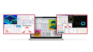

Validate Your Design Using RF Simulation

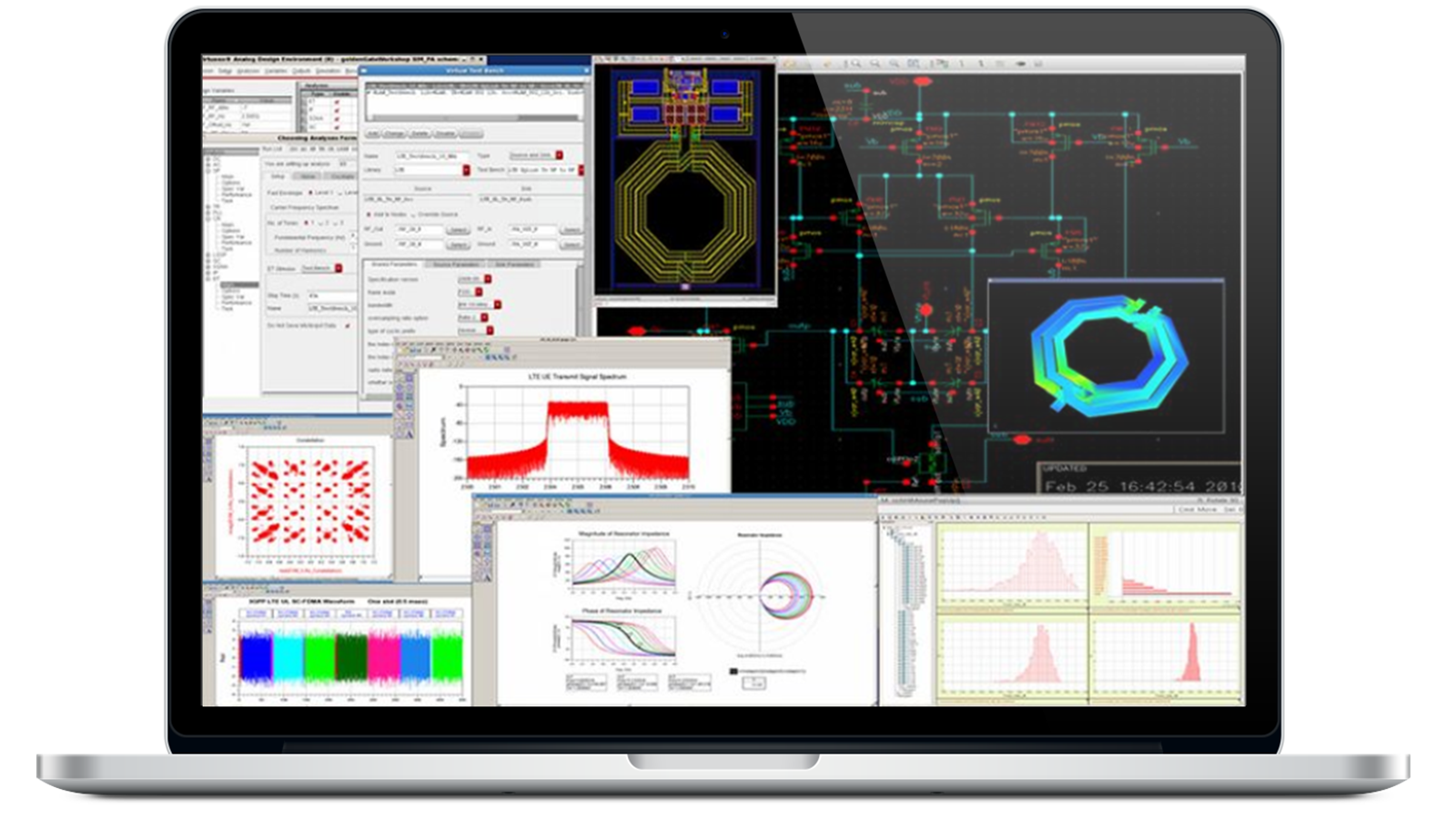
Electronic design automation (EDA) tools simulate and validate a circuit design before and during board layout. EDA tools can be used for chip, module, board, and system-level design and help you deal with the complexity of modern RF applications, especially in the microwave and millimeter-wave spectrum.
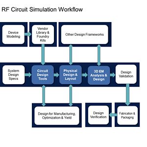
EDA workflow has become critical for interoperability between the tools and ensuring an accurate and efficient simulation. The workflow diagram at the left shows the functional blocks of the design process – where the blue blocks represent the core of RF design simulation. The circuit design tool allows you to enter the schematic and perform simulations on many key signal performances. The physical design and layout enable you to lay out the tracks and components on the board and simulate transmission line properties like impedance and crosstalk. The 3D electromagnetic (EM) analysis and design allow you to simulate how the product will perform on a system level.
To design an RF low noise amplifier (LNA), a typical use case is to run an RF simulation on the schematic to ensure that the gain, noise, and frequency response are acceptable. The board layout introduces additional variables such as the layer stackup and dimensions of tracks, which also require simulation. Finally, EM analysis lets you simulate the performance of your final product as it relates to regulatory compliance.
Prolonged design cycles?
Simulate Your Design Iteratively During the Design and Prototype Phases
Different tools slowing you down?
Use EDA Solutions That Are Natively Interoperable and Compatible
Excessive crosstalk and power loss?
Use EM Simulation to Identify and Correct Crosstalk and Power Loss
Keysight RF Circuit Simulation Solution
With the Keysight RF circuit simulation solutions, you can quickly accelerate your RF design validation using wizards and templates.


Watch the RF Circuit Simulation Solution Demo
Learn More About RF Circuit Simulation
Discover how to use look-a-like components directly in an ADS schematic
Learn how to use ADS to characterize, optimize, and layout your design
Explore how GoldenGate can simulate, verify and analyze your design
Additional Resources


Want help or have questions?