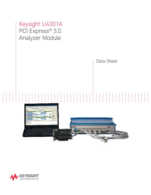
U4301A PCI Express® 3.0 Analyzer Module
Data Sheets
Data Sheet
Introduction
Keysight solutions for PCIe Gen1 to Gen3 analysis and emulation.
- PCI Express generation 1, 2, & 3 protocol architecture
- Lane speeds 2.5 GT/s, 5.0 GT/s, and 8.0 GT/s
- Lane widths x1, x4, x8, and x16
- Stimulus response testing with the addition of the U4305A protocol exerciser
- NVMe device analysis and emulation
- Compact AXIe modular system configuration
Overview
Product Description
Keysight Technologies’ high speed U4301A PCI Express® 3.0 analyzer module is a protocol analyzer supporting all PCI Express® applications from Gen1 through Gen3 and speeds, including 2.5 GT/s (Gen1) and 5.0 GT/s (Gen2) through PCIe 8 GT/s (Gen3) and with link widths from x1 to x16. The U4301A analyzer captures and decodes PCI Express data and displays it in a packet viewer window.
The U4301A analyzer is a blade that is installed in an AXIe two slot M9502A or five slot M9505A.
Probing is provided by the U4321A solid slot interposer probe, U4324A flying lead solder down probe, or the U4322A mid bus probe based on Keysight’s equalization snoop probe (ESP) technology.
Stimulus and response testing of the PCIe system is accomplished with the addition of the U4305A PCIe Gen3 exerciser.
A link training status state machine (LTSSM) exerciser provides stimulus for testing PCIe links up to the full speed of Gen3 systems. The analyzer LTSSM overview can pinpoint specific training sequence issues through easy to interpret analysis results.
Keysight’s Transactional decoder includes a transactional viewer that allows the designer to select transactional queues and performance information from the analyzer’s NVMe transaction overview pane.
This organizes the transactions by direction or by queue to follow the data flow across the interface, with one-click control. Individual PRP (Physical Region Page) lists contain all of the key information of the NVMe queues, allowing designers to quickly review and validate the data flows over the PCIe connections.
The Performance analysis package includes the real data throughput calculations, with response-time measurement of the PCIe data flow. It allows designers to measure and understand throughput performance, PCIe response times, and other operational measurements that provide the insight needed to optimize device performance.
Analysis and debug
- Support for Gen1 through Gen3, x1 through x16 link width
- 4 GB of capture buffer per module
- Non-intrusive probing that leverages ESP technology
Industry leading probes
- The mid-bus probe supports x1 to x16 unidirectional or x1 to x8 bidirectional
- The solid slot interposer will support x1 to x16 unidirectional or bidirectional
- The flying lead solder down probe offers support for x1 & x2 bidirectional capability on a single probe. Other standard lane width configuration support is x4, x8, & x16
Stimulus and test U4305A exerciser
- Support for Gen1 through Gen3 and link widths of x1 through x16
- Link testing from x1 through x16, using automated LTSSM exerciser
- PCIe, MR-IOV, and SR-IOV stimulus response testing
- INVMe Root Complex emulation for test and verification of NVMe devices
- Protocol test card (PTC) to measure PCIe Gen3 DUT port and system BIOS specification compliance as defined by the PCI SIG standards
Product Features and Benefits Overview
U4301A analyzer module
Effective presentation of protocol interactions from physical layer to transaction layer
- LTSSM Overview with full state transaction traffic capture at the PHY layer logic sub block
- Industry standard spreadsheet format protocol viewer with:
- Highlighting by packet type or direction
- Easy flow columns to better understand the stimulus and response nature of the protocols
- Context sensitive columns to show only the relevant information, minimizing the need to scroll horizontally
- Flexible GUI configuration to meet debug needs, with pre-defined GUI layouts for link training debug, config accesses and general I/O