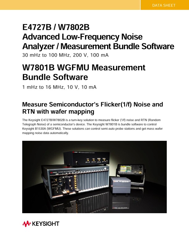
E4727B/W7802B Advanced Low-Frequency Noise Analyzer/Measurement Bundle Software
Data Sheets
Measure Semiconductor's Flicker(1/f) Noise and RTN with wafer mapping
The Keysight E4727B/W7802B is a turn-key solution to measure flicker (1/f) noise and RTN (Random Telegraph Noise) of a semiconductor's device. The Keysight W7801B is bundle software to control Keysight B1530A (WGFMU). These solutions can control semi-auto probe stations and get mass wafer mapping noise data automatically.
Introduction
Electrical noise is inherent in every circuit and may be caused by current flowing through a resistor or transistor, or even leakage current through a tantalum capacitor. As a classical limitation of electronics, this noise must be managed. A systems engineer must understand the overall system sensitivity to noise, and then derive the key contributors. A typical key contributor might be a component like a semiconductor device, sensor, or passive component. How do we quantify the noise of these constituent parts? The Keysight E4727B Advanced Low-Frequency Noise Analyzer (A-LFNA) enables a closer, deeper look at noise in components, individual devices, and integrated circuits, both packaged and at the water level. A device modeling engineer may now leverage the A-LFNA’s rare combination of industry-leading noise sensitivity (-185 dBV2/Hz) to characterize devices at high voltages (to 200 V) and down to ultra-low frequencies (to 30 mHz). Thanks to seamless integration with PathWave WaferPro Express software, one may program and sequence high-speed DC, capacitance, and RF measurements, all the while automating wafer prober control. The resulting noise data may be used to develop device models with the help of state-of-the-art device modeling tools like Model Builder Pro (MBP) and Integrated Circuit Characterization and Analysis Program (IC-CAP). These models can then be passed along to circuit designers, who may then push the envelope in low-noise circuitry.
The applications for wafer-level 1/f noise measurements are numerous; however, a few important ones are listed as follows.
• Process design kit development. Semiconductor device foundries enable fabless design centers to design components such as transceivers for mobile phones, frequency synthesizers, analog-todigital converters, and much more. To make this possible, the foundries must provide Process Design Kits (PDKs) with simulation models of the primitive devices. The simulation models must include noise effects on transistors (BJT, CMOS, etc.) and resistors. The noise models must be across all possible bias currents, temperatures, and device geometries.
• Manufacturing statistical process control and reliability. As an example, manufacturers of GaN devices may use noise measurements across their wafers as an early indicator of device reliability. Those devices that exhibit more noise are likely to fail sooner. Now we have a nondestructive way of assessing reliability, quite in contrast with standard accelerated life testing. Furthermore, for circuit applications where noise is a critical parameter, wafer-level measurements may be used to track the evolution of noise performance across days, weeks, and months of manufacturing.
• IC noise specification. Integrated circuit manufacturers of operational amplifiers and linear voltage regulators often need to characterize input referred voltage noise as a critical specification in their datasheets. One wafer may contain > 10 thousand such circuits. To efficiently measure and map circuit performance across the wafer (and even across lots of wafers), the probe and signal conditioning circuitry must be placed close to the device under test to improve grounding and minimize external noise influences.