What are you looking for?
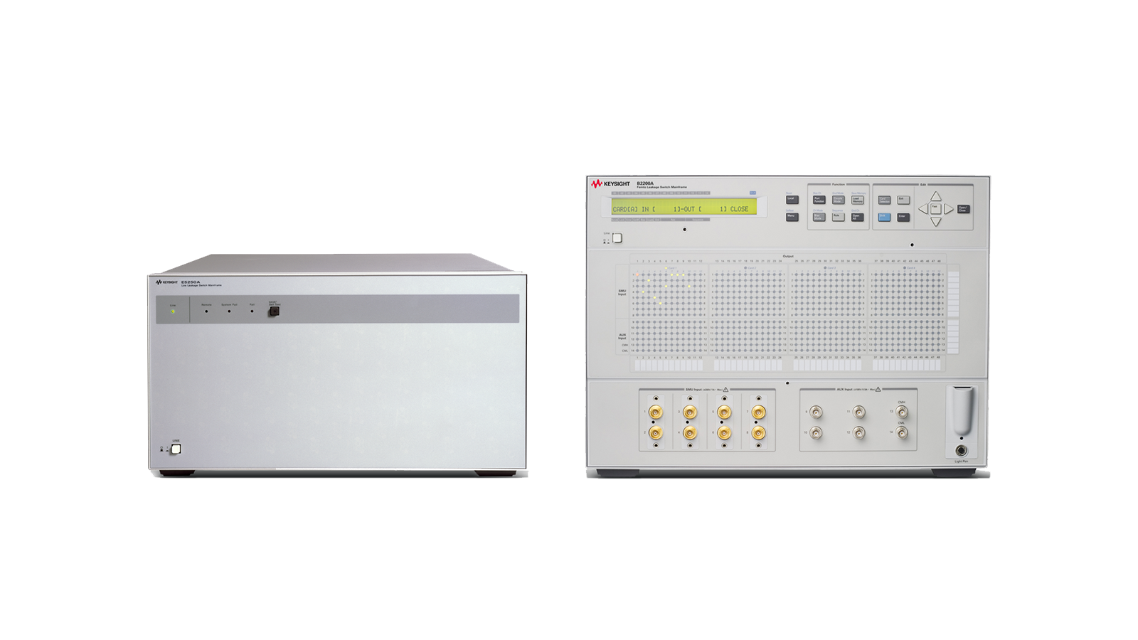
Low-Leakage Switch Matrix Family
Reduce cost of test through characterization test automation

Challenges
Making parametric measurements necessary for the numerous test structures on a semiconductor wafer is a time-consuming and expensive process. With the cost of end-user devices continuing to drop, even laboratory characterization environments must reduce the cost of test.
Using a switching matrix with a semi-automatic or fully-automatic wafer prober enables automation of characterization tests eliminating the need to have an operator manually reposition the probes each time a new module requires testing.
Get flexible switching matrix options
You can choose only the capabilities your testing needs require, nothing more. The solution contains multiple options for current measurement resolution and input / output configurations. The solutions include a powerful feature to compensate for the capacitance measurement distortion created by the matrix's internal path lengths.
Choose the measurement resolution that best matches your needs
Choose between 1 fA and 10 fA current measurement resolution — the switching matrix keeps pace with your semiconductor parameter analyzer's capabilities without loss in measurement performance caused by signal leakage.
Flexible input and output configurations
Available options span the continuum of cost and performance, from cost-effective measurement solutions for non-Kelvin measurement up to 4-SMU, full-Kelvin measurement configurations. You can select a variety of output channel configurations and card types to meet your measurement needs.
Make accurate capacitance measurements without distortion
Keysight's switching matrices have a capacitance measurement compensation feature that corrects the error introduced by the matrix's internal path lengths. This solution makes accurate capacitance measurements through a switching matrix to give you compensation parameters to enable undistorted measurement results.
Find the Model That's Right for You
Protect Your Innovation Investment
Featured Resources
Want help or have questions?


