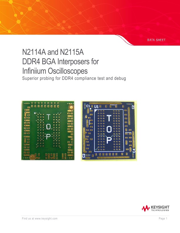
N2114A and N2115A DDR4 BGA Interposers for Infiniium Oscilloscopes
Data Sheets
N2114A and N2115A
DDR4 BGA Interposers for Infiniium Oscilloscopes
Superior probing for DDR4 compliance test and debug
Introduction
The DDR4 BGA interposers provide signal access to clock, strobe, data, address and command signals of the DDR4 BGA package for making electrical, timing and eye diagram measurements with an Infiniium oscilloscope. The DDR4 JEDEC1 specification is defined at the DRAM ballout, and the ballout is difficult to access. The BGA interposer provides direct signal access to the BGA package for true compliance testing.
The DDR4 BGA interposers are soldered between the DRAM and PC board or DIMM raw card where the DRAM would normally be soldered. They are designed with the PCB or DIMM footprint on the bottom side and the DRAM footprint on the top side. The BGA interposer passes the signals from the memory controller chip and DRAM directly to the top side of the BGA interposer where they can be accessed with oscilloscope probes.
Buried resistors placed at the signals inside the BGA interposer connect the probed signals to solder pads designed to work with InfiniiMax differential or single-ended solder-in probe heads. These resistors isolate the DDR4 signal and the probe loading effect. This design minimizes capacitive loading of the probe heads and allows high-speed operation without impact on signal integrity.
Probing at the right location is also an important consideration for DDR4 measurement. Many designs have vias or designed-in probe points, but they do not always produce good signal integrity. Probing at the wrong location could cause signal reflection, resulting in non-monotonic edges. This will cause error in your tests such as slew rate, setup and hold time measurements.
When used with N6462A/B DDR4 compliance test application, the BGA interposers provide a fast and easy way to test, debug and characterize your DDR4 designs. The tests covered by the N6462A/B software are based on the JEDEC DDR4 SDRAM specification. The test application offers a user-friendly setup wizard and a comprehensive report that includes margin analysis.
Features
- Provides signal access points for DDR4 DRAM x4, x8 and x16 packages using JEDECstandard common BGA footprints to the oscilloscope
- Buried resistors provide signal isolation and minimize capacitive loading
- Perimeter solder-down test points can be used with Logic Analyzer flying leads or Oscilloscope solder-down probe tips to access signals
- Effective bandwidth may be extended with InfiniiSim Waveform Transformation software
- Measurement timing skews reduced by matched trace lengths from DDR4 balls to test points
- Capacitive decoupling of the power and ground is achieved with plane layers within the stackup of the interposer and four SMT capacitors
- Probing compatibility with InfiniiMax probe, which includes E2677A, N5381A, and N5425A/N5426A differential solder-in probe heads
Installing the DDR4 BGA interposer
The DDR4 BGA interposer is installed by soldering onto the BGA footprint of the PC board or DIMM card where the DRAM normally would be soldered. Then, solder the DDR4 DRAM to the top side of the BGA interposer. A riser may be soldered below the interposer to provide a lift to avoid interference with the adjacent components on the board or DIMM. These attachment steps may occur in any order.
The probe is designed to tolerate lead-free soldering temperature profiles. However, we recommend you apply the minimum temperature required for soldering and use the minimum number of heating and cooling cycles to reduce risk of any damage to the probe. The probe is supplied with lead-free solder balls.
We recommend you attach the BGA interposer during the manufacturing process. For designs that are manufactured, it will require expertise to attach the BGA interposers. If you lack the in-house expertise to attach the BGA interposer, you may wish to work with a contract manufacturer with this expertise that may be willing to perform the attachment for a fee. You can find more information on BGA soldering and rework techniques that may be useful in attaching the probe at: http://www.circuitrework.com/guides/9-1-1.shtml